Snapdragon 8 Elite Gen 5 Explained: CPU, GPU, AI, and Efficiency Full Breakdown
The chip Qualcomm announced on September 25, 2025 carries a new number and a new name convention—and that combination has already produced more confusion than clarity. It is not called the Snapdragon 8 Elite 2. It is not a minor refresh. The Snapdragon 8 Elite Gen 5 (SM8850-AC) represents a full generational jump: a new CPU microarchitecture, a new GPU feature set, a redesigned neural processing pipeline, and a process node transition that lands simultaneously with Apple’s A19 Pro on TSMC’s 3nm-class silicon. The Samsung Galaxy S26, Xiaomi 17 Pro, and Sony flagship devices announced in late 2025 all run on it. What it actually delivers under those marketing claims is a different, more complicated story.
- The Oryon Gen 3 CPU delivers 20% higher peak throughput and 35% better power efficiency than its predecessor, per Qualcomm’s September 25, 2025 announcement at the Snapdragon Summit in Maui, Hawaii.
- The Adreno 840 GPU adds hardware ray tracing (+25% gen-over-gen) and Vulkan 1.4, yet Apple’s A19 Pro draws 42% less power per Geekbench 6 multi-core point under sustained load, according to Geekerwan power testing reported by WCCFtech in September 2025.
- “100 TOPS NPU” is a peak theoretical ceiling—real AI throughput depends on whether the workload uses Hexagon-optimised operators; models not targeting Qualcomm’s AI Engine SDK fall back to the CPU or GPU.
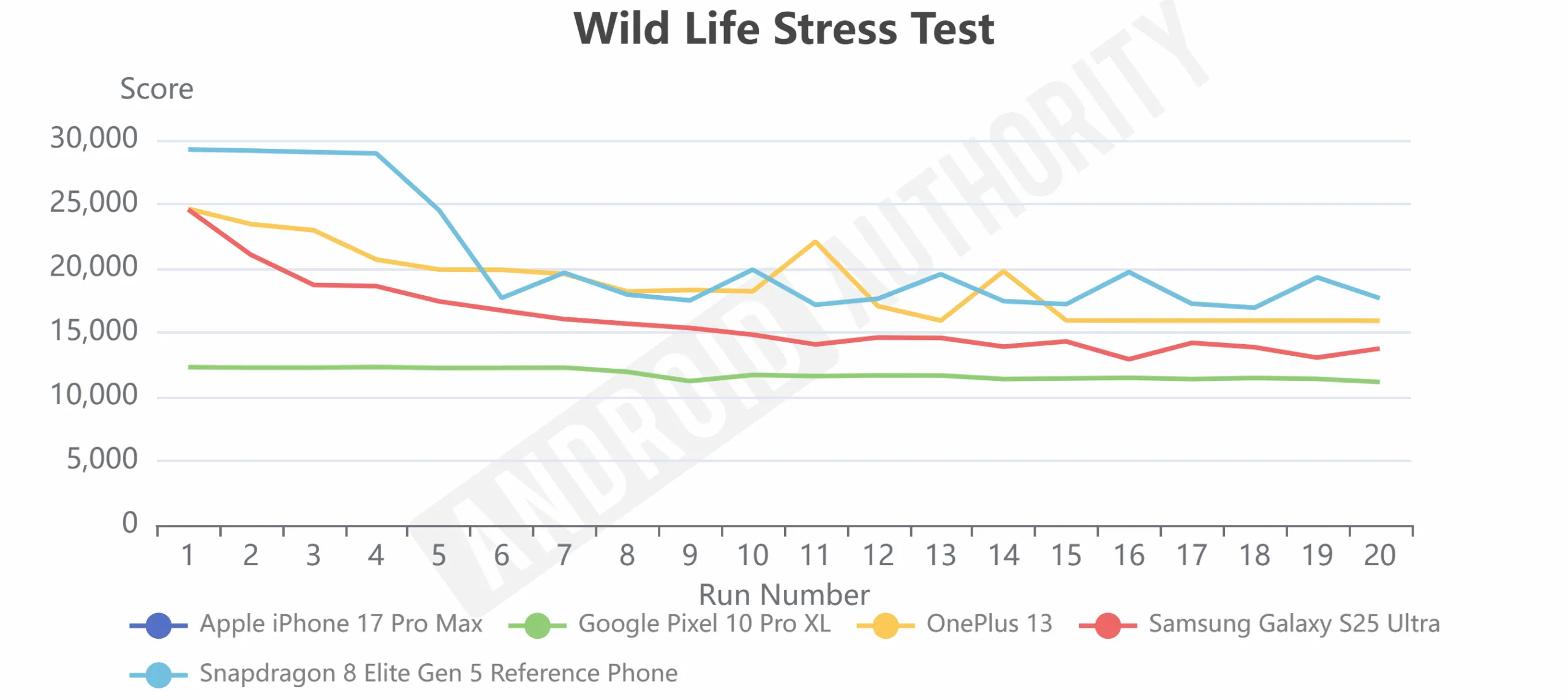
- Under a sustained 3DMark Wild Life Stress Test, throughput collapsed to 58% of peak after four full runs on Qualcomm’s own reference device (Android Authority, September 2025)—the host phone’s cooling design determines real-world sustained performance.
- The SM8850-AC is the first mobile platform to support the Advanced Professional Video (APV) codec, enabling 10-bit 4:2:2 recording workflows previously confined to dedicated cameras.
Last updated: 2025-09-30 · Sources linked inline
The Snapdragon 8 Elite Gen 5 (SM8850-AC) is Qualcomm’s 2025 flagship mobile SoC, built on TSMC’s 3nm N3P node. It pairs a third-generation Oryon CPU in a 2+6 configuration—two prime cores at 4.6 GHz and six performance cores at 3.62 GHz—with an Adreno 840 GPU, a 100 TOPS Hexagon NPU, and the world’s first mobile APV codec implementation. Generation-over-generation gains measure 20% CPU performance, 35% CPU efficiency, 23% GPU performance, and 37% NPU speed, per Qualcomm’s September 25, 2025 announcement.
Contents
Snapdragon 8 Elite Gen 5 Explained: The Short Version
Every Qualcomm flagship since the original Snapdragon 8 Gen 1 has followed the same basic architecture: one cluster of power-hungry prime cores, one cluster of performance cores, one efficiency cluster. The Elite Gen 5 drops the efficiency cluster entirely. What replaces it is a 2+6 configuration—two Oryon Gen 3 prime cores running at 4.6 GHz and six performance cores at 3.62 GHz—where Qualcomm claims the performance cores are individually efficient enough to absorb what three tiers previously handled. That structural decision is what enables the 35% efficiency gain on the CPU side: the workload routing logic no longer needs to manage three core types, and the performance cores themselves run on a significantly revised pipeline with wider execution windows.
Surrounding the CPU are four distinct functional blocks that matter independently: the Adreno 840 GPU, the Hexagon NPU, the Spectra AI ISP, and the Snapdragon X85 5G modem. Each block gets its own clock domain, power gate, and memory interface. The system-level cache—8 MB of shared SRAM sitting between all blocks and the LPDDR5X memory controller—is the traffic hub that makes the whole architecture function as a coherent unit rather than four separate processors sharing a bus.
Why “Gen 5” and not “Elite 2”
Qualcomm quietly retired its sequential numbering convention for the Elite line. The SM8850-AC succeeds the SM8750-AB Snapdragon 8 Elite, but Qualcomm chose “Gen 5” to align the suffix with the internal silicon generation of the Oryon core series—the same numbering that governs Snapdragon X Elite chips in the PC market. That Oryon lineage continues in the Snapdragon X2 Elite, making “Gen 5” a cross-platform identifier rather than a simple marketing increment. Qualcomm confirmed this naming rationale directly in a September 2025 blog post, writing that the Gen 5 suffix “reinforces its leadership position and simplifies how consumers understand our product roadmap.”
How the Snapdragon 8 Elite Gen 5 Actually Works
The CPU: what the 2+6 configuration actually changes
The two prime Oryon cores run at 4.6 GHz—a figure high enough that thermal headroom, not transistor budget, is the real limiting factor at peak. Under Geekbench 6 single-core testing on Qualcomm’s reference device at the Summit, Android Authority confirmed single-core gains of approximately 19% over the prior Snapdragon 8 Elite. That number places the chip ahead of the previous Elite in single-thread, and nearly level with Apple’s A19 Pro in the same test—less than 1% separates them, according to Android Authority’s hands-on benchmark session in September 2025. The six performance cores at 3.62 GHz are where the story gets more interesting: they handle the sustained multithreaded workloads that represent the majority of real usage, and they achieve the 35% efficiency improvement Qualcomm cites by running at a wider issue width than the Gen 4 cores while retiring instructions faster per clock cycle.
In multi-core, the Snapdragon 8 Elite Gen 5 actually surpasses Apple’s A19 Pro—by approximately 25%, per Android Authority’s September 2025 reference-device testing. The critical caveat: the Snapdragon consumes approximately 19.5 watts during that multi-core run compared to the A19 Pro’s 12.1 watts, according to Geekerwan power measurements reported by WCCFtech on September 25, 2025. That is a 42% efficiency gap per performance point. The Snapdragon wins absolute throughput; Apple wins absolute efficiency. Readers building battery-life-first Android flagships should note that tradeoff before citing the headline multi-core number.
What most explanations skip: the SLC is not L3 cache
Multiple benchmark write-ups in September and October 2025 described the Snapdragon 8 Elite Gen 5’s 8 MB shared memory as “L3 cache.” That is architecturally inaccurate. The 8 MB SLC (System Level Cache) sits outside the CPU complex and is shared between the CPU, GPU, and NPU. Each individual Oryon core retains its own private L1 and L2 caches. The SLC provides a last-level landing zone before requests escalate to LPDDR5X main memory. The practical consequence is that GPU and NPU workloads can reuse CPU-loaded data without a round trip to DRAM—a bandwidth saving that contributes to the 38% HPM cache bandwidth improvement confirmed by Jon Peddie Research in their November 2025 analysis.
GPU and gaming stack
The Adreno 840 name did not appear in Qualcomm’s official press release at the Summit—the company referred only to “Adreno GPU” throughout—but Jon Peddie Research confirmed the Adreno 840 designation in their November 2025 analysis. The GPU supports Vulkan 1.4 and DirectX 12, adds a hardware ray tracing block that delivers 25% more RT throughput than the previous Adreno, and introduces Tile Memory Heap and Mesh Shading as distinct rendering features for Unreal Engine 5 content. Tile Memory Heap reduces bandwidth by keeping intermediate render data on-chip during a tile-based rendering pass rather than flushing it to DRAM. Mesh Shading allows developers to cull geometry on the GPU before the rasteriser ever sees it, removing the fixed-function vertex pipeline bottleneck for complex scenes.
Android Authority’s hands-on 3DMark testing at the Summit found GPU performance improvements between 15% and 18% depending on the workload—more conservative than Qualcomm’s quoted 23%, but the reference device’s 24 GB LPDDR5X configuration represents conditions no retail phone will replicate. The 20% power efficiency improvement Qualcomm cites for the GPU applies specifically to sustained rendering workloads where the Tile Memory Heap actively reduces DRAM traffic. Workloads that bypass the tiling pipeline—certain compute shaders and GPU ML inference tasks—will see smaller gains.
The Hexagon NPU and agentic AI
Qualcomm’s use of “agentic AI” throughout the Summit keynote describes a specific capability: the Hexagon NPU, paired with the Qualcomm Sensing Hub, can run persistent background models that monitor sensor inputs and proactively modify application behaviour without a user initiating a query. Whether you want that persistent inference running is a separate question. The NPU itself peaks at 100 TOPS and is 37% faster generation-over-generation. Android Authority’s MLPerf results from the Summit showed real-world AI gains ranging from 19% (image classification) to 55% (super-resolution) depending on the specific task—confirming that the 37% headline figure is a midpoint, not a floor.
Common Misconceptions About the Snapdragon 8 Elite Gen 5
“More TOPS always means better AI performance”
100 TOPS is a theoretical maximum computed under conditions that no real application reproduces: full utilisation of all MAC units, running a supported precision format, with perfectly tiled data. Every AI inference workload that reaches a device runs through an operator library. If that operator is not Hexagon-optimised, the computation falls back to the CPU or GPU, where the TOPS figure is irrelevant. Android Authority explicitly noted in their September 2025 analysis that the chip’s NPU performance depends critically on “developers spending time in chipset-specific API libraries.” The new INT2 precision support extends the range of models that can run on-device, but at accuracy trade-offs that vary by model architecture. The number to watch is tokens per second or milliseconds per inference for your specific model family—not headline TOPS.
“The Snapdragon 8 Elite Gen 5 is the Snapdragon 8 Elite 2”
This naming confusion was not user error—it was genuinely ambiguous before the Summit. Qualcomm had used “Gen 2” nomenclature in pre-release documentation visible in several August 2025 Geekbench database entries. The official name announced September 25 is “Snapdragon 8 Elite Gen 5,” with the “Gen 5” suffix tracking the Oryon microarchitecture generation rather than the Elite product line generation. The chip before it—SM8750-AB—is now retroactively referred to as Snapdragon 8 Elite (Gen 4) in technical contexts. Search queries for “Snapdragon 8 Elite 2” or “Snapdragon 8 Gen 5 Elite” continue landing on wrong results as a consequence.
Real-World Applications
Gaming and sustained performance
The AnTuTu V11 score exceeding 3.7 million represents a headline figure that breaks records but obscures the throttling reality beneath it. Android Authority’s 3DMark Wild Life Stress Test on Qualcomm’s own reference device—running under optimal Summit conditions with a 24 GB LPDDR5X configuration—saw throughput collapse to 58% of peak after four full runs. Qualcomm claims the overall efficiency improvement equates to 1 hour and 48 minutes of additional gaming time, a figure derived from platform-level power reduction rather than any specific retail device test. For flagship gaming devices like the Samsung Galaxy S26 Ultra, which uses a vapour chamber thermal solution, sustained performance will differ substantially from a thin mid-range slab using the same chip.
Photography and the APV codec
The Spectra AI ISP is where the Snapdragon 8 Elite Gen 5 has its most unambiguous advantage over any current alternative. Triple 20-bit AI-ISP pipelines (upgraded from 18-bit on the prior generation) running in parallel allow simultaneous RAW capture, multi-frame processing, and real-time AI segmentation without serialising operations through a single pipe. The APV codec support makes this the world’s first mobile platform with APV capability, enabling 10-bit 4:2:2 intra-frame recording. That matters specifically for post-production workflows: 4:2:2 colour sampling retains twice the chroma data of 4:2:0 at the same spatial resolution, which is the difference between clean colour grading and visible blocking artefacts in sky gradients. However, as Android Authority noted in September 2025, APV requires encoder support from every downstream application—and at launch, no major editing platform had published confirmed APV compatibility timelines.
Productivity and on-device AI
On-device LLM inference at INT4 quantisation is now practical at 13 billion parameters—a threshold that covers models like Llama 3.1 13B. The Qualcomm Sensing Hub adds persistent background context: location, activity, ambient sound classification, and calendar state can be fed continuously to a small on-device model without waking the main CPU cores. The practical limit is memory bandwidth. At LPDDR5X bandwidth—approximately 68 GB/s on typical implementations—a 13B INT4 model requires roughly 7 GB of model weights to be streamed per inference pass. Whether OEMs ship 16 GB LPDDR5X configurations will determine whether this feature is accessible in practice. Devices shipping with 12 GB will face operational constraints on the largest on-device models.
Snapdragon 8 Elite Gen 5 vs Dimensity 9500
| Dimension | Snapdragon 8 Elite Gen 5 | Dimensity 9500 |
|---|---|---|
| CPU configuration | Oryon Gen 3, 2+6, 4.6 GHz prime | Cortex-X930 + A720, 1+3+4, 3.62 GHz |
| Process node | TSMC N3P (3nm) | TSMC N3E (3nm) |
| GPU | Adreno 840, Vulkan 1.4, DX12 | Mali-G1 Ultra, Vulkan 1.3 |
| NPU peak | 100 TOPS | 35 TOPS |
| Ray tracing | Hardware-dedicated block | Software-assisted |
| APV codec | Yes (world-first) | No |
| Memory | LPDDR5X × UFS 4.1 | LPDDR5X × UFS 4.0 |
Key differences: The Snapdragon’s Oryon CPU architecture and hardware ray tracing make it the clear choice for developers targeting Vulkan 1.4 rendering pipelines and UE5 content. The Dimensity 9500’s Mali-G1 Ultra GPU performs competitively in rasterised workloads according to NotebookCheck’s November 2025 analysis, but loses ground specifically in ray tracing scenarios because its implementation is software-assisted rather than silicon-dedicated. Buyers on MediaTek-based devices—primarily Vivo, OPPO, and select Xiaomi models—who do not play ray-traced titles and are indifferent to the APV codec have no technical reason to pay a premium for Snapdragon-based alternatives. The Dimensity 9500 is a legitimate competitor on TSMC 3nm; it is not inferior across every use case.
What the Future Looks Like
Two developments are in confirmed active development as of late 2025. First, Qualcomm has publicly disclosed the Snapdragon X2 Elite for PC, which shares the Oryon Gen 5 microarchitecture with the SM8850-AC. That platform brings the same CPU generation into laptop form factors in 2026, meaning compiler and runtime optimisations developed for mobile will transfer without re-certification. Second, Qualcomm confirmed at the Summit that on-device agentic AI features require firmware updates from OEMs to unlock; the NPU hardware is present in all SM8850-AC units, but the Qualcomm Sensing Hub integration layer ships as a software activation. The OEM firmware rollout timeline has not been formally confirmed by Qualcomm as of September 2025.
What remains genuinely unresolved: whether APV will achieve broad app support within the first device generation, and whether the Snapdragon 8 Elite Gen 5 for Galaxy—Qualcomm’s binned variant for Samsung—will hit the rumoured 4.74 GHz prime core frequency. The codec hardware exists in the SM8850-AC; the ecosystem supporting it does not yet. No major video editing platform had published confirmed APV compatibility timelines as of this writing. First-generation features with thin ecosystem support have historically taken 12–18 months to become genuinely usable—as Arcsoft’s Video Magic Eraser, introduced with an earlier Snapdragon generation, demonstrated by seeing near-zero OEM adoption.
Frequently Asked Questions
What is the Snapdragon 8 Elite Gen 5?
How does the Snapdragon 8 Elite Gen 5 compare to the Apple A19 Pro?
What phones use the Snapdragon 8 Elite Gen 5?
Is the Snapdragon 8 Elite Gen 5 better than the Dimensity 9500?
Does the Snapdragon 8 Elite Gen 5 overheat?
What is the Hexagon NPU in the Snapdragon 8 Elite Gen 5?
The Bottom Line
The Snapdragon 8 Elite Gen 5 is the most capable Android SoC announced in 2025 on every directly measurable metric: single-thread CPU, multi-thread CPU, GPU rasterisation, hardware ray tracing, NPU throughput, and imaging pipeline depth. It is also a chip that demands evaluation in context. It draws more power than Apple’s A19 Pro per performance unit. Its top benchmark scores require thermal conditions that most retail devices cannot sustain beyond 15 minutes of continuous load. Its most distinctive new feature—the APV codec—has an ecosystem that does not yet match the hardware capability. Those are real limitations, not dismissals. For users building a premium Android workflow around professional video, gaming, and on-device AI inference, this generation of the Snapdragon platform is meaningfully ahead of its immediate predecessor and every competing Android chip.
The right question before selecting a device is not whether the Snapdragon 8 Elite Gen 5 is “the best chip”—it is whether the specific device housing it has thermal management capable of sustaining its performance tier, and whether the software you use has been optimised for its NPU and GPU feature set. A well-cooled Dimensity 9500 device will outperform a thermally compromised Snapdragon 8 Elite Gen 5 phone in any workload that runs longer than ten minutes. The same cooling-versus-silicon principle applies across Snapdragon platforms—the chip’s ceiling only matters when the device is built to reach it. For flagship buyers evaluating the Galaxy S26 series, the Snapdragon 8 Elite Gen 5 is unambiguously the right foundation—provided Samsung’s vapour chamber keeps it running near its ceiling.